
Disclaimer This is my first real electronics, hardware project. I'm picking this up as I go. I don't yet have a mature mental model on electronics. I appreciate any guidance and coaching in the comments.
Building a DIY E-ink or Epaper laptop
This is a follow up to my previous Dasung Paperlike Pro Review post. For visitors landing here, a quick recap. The Dasung Paperlike Pro is billed as "The worlds first HDMI e-ink monitor" It is high performance for a e-ink display and renders at about 40fps. Check the review post for more info.
I Bought the Dasung with intentions to tear it down for 'research' purposes. Mainly to confirm what e-ink display module they were using. This research was for the goal of building an e-ink laptop. In this post I will walk through my experience dismantling the Dasung and discuss its internal components. Hopefully readers will find this useful in their own e-ink hardware projects, or in the chance they need to repair a Dasung.
You can click through any of the images below for full high res versions.
How to open the Dasung Paperlike Pro
The Dasung has a seemingly, solid one piece construction. It took me a few days to devise a method of disassembly that wasn't aggressively destructive, like cracking the frame open with a hammer, or pry-bar. After prodding it for a few days I discovered the front outer frame bezel was glued on and could be pried with a knife.


The Dasung E-ink display module
My main objective in purchasing the Dasung, was to confirm what e-ink display module was in use. I had suspected it was the 13.3˝ ePaper Display (ED133UT2) However other notes from Dasung about a "Carta" version change lead me to doubt that. One of my biggest complaints in my Dasung Paperlike Pro Review post, was that the monitor display was reflective and has an aggressive glare.
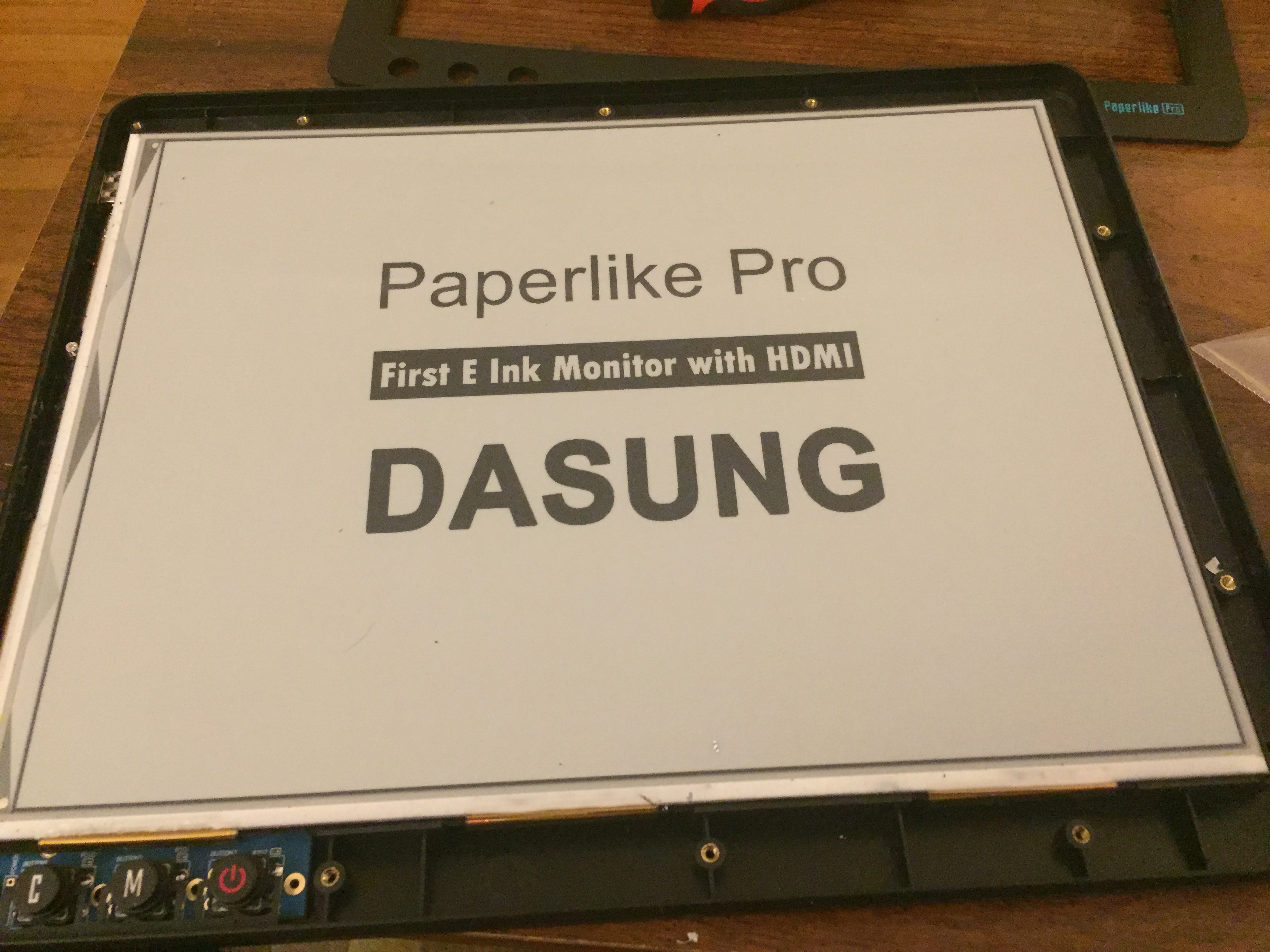
Detaching the E-ink display module
This step was sensitive. The Display module is attached by a fragile ribbon cable to a latch bracket. This is called a ZIF (Zero Insertion Force) connector. It took me a bit to track down how to open it. You Lift the black latch off and can remove the ribbon cable.
 connector")
Reviewing the E-ink Epaper display module
On inspection of the E-ink display module I was disappointed to find that the glass was actually part of the module and not a separate pane like I first expected and hoped.


The tag on the display module has a model number ED133UT2 that confirms my suspicious of it being the e-ink 13.3 ed133ut2. This is unfortunate as it appears that E-ink offers another module the ES133UT2 model. Note that the difference between the model numbers is the S and D. The S model is marketed as "Flexible" and has sales points of:
- Antiglare hard-coated front-surface
- Plastic substrate
It is hugely disappointing that Dasung went with the D model as I suspect the S model would be an anti-glare e-ink display module solving a major problem with the Dasung. I could almost see a mistake being made during production ordering because of the very close model identifiers.
On further exploration of these model numbers I found a PaneLook.com a whole sale display panel site which lists other 13.3 e paper, display models:
- EN133UT1
- ES133UT1
- ED133UT1
- ED133TT1
- ES133TT2
- ES133TE1
- ED133UT2
- ES133TT3
Panelook curiously does not have a listing for ES133UT2
A comparison of 13.3 epaper displays on PaneLook shows some interesting details about the available options.
- The ES133TE1 has embbed touch screen capabilities.
- EN133UT1 and ES133TT3 are the only models listed with 'Antiglare'
After comparing these options it looks as if ES133TT3 would be the best Epaper laptop display from these options.
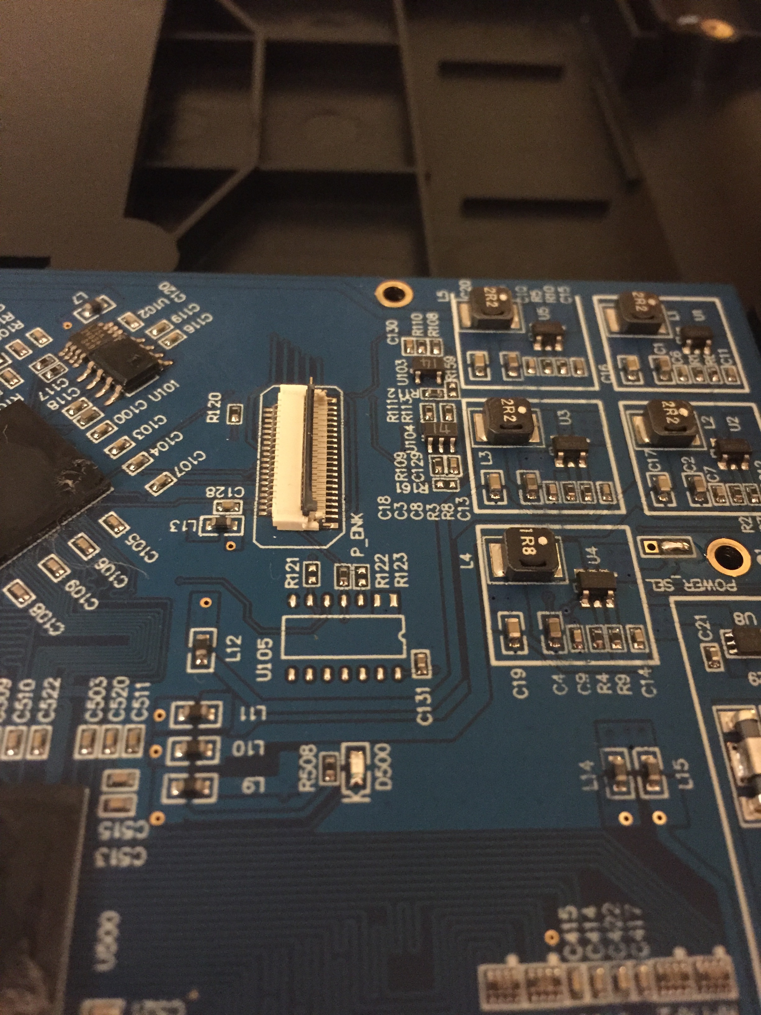
The Control Board
When I first saw this control board I was shocked at how large it is and how many components are packed into it. I had assumed that most of the proprietary Dasung functionality was handled in software.

On closer inspection all the chip components have had their labels chemically peeled off to prevernt reverse engineering.
Two PCBs ?
There are actually two PCBs. A smaller PCB towards the top of the enclosure is a USB port with an IC and wires hooked to the main board.

The Dasung manual claims that this USB port is intended to be used as an interface for a USB external lamp. Then elsewhere, on the included accessories section of a 'quick start' sheet, it says:
- A USB to USB cable for firmware upgrade in some emergency (non standard).
This implies that the USB interface can used for firmware updates. I suspect with some further hacking this could be used to load custom firmware or maybe dump the existing firmware of the board.
There are only two input ports to the device. The USB on top, and the mini HDMI in the bottom left.
Dasung Paperlike Pro control board components
I am way too junior in electronics to accurately identify the components of the board. I leave this as an exercise for any readers, and a learning challenge for myself. I will pursue this in future work.
I reached out to some 3rd party help and the best lead I got was:
from top to bottom... some kind of IO breakout, maybe an MCU for platform management, might actually be running the whole show and below is just a display controller main SoC, probably contains display driver they're using for just the internal screen the two little ones are DRAM an FPGA, used as glue logic and DMA buffer for both displays highly integrated hdmi controller, handles the full spec + audio and just clocks in a frame
the collection of shit in the white boxes are various power regulators for the display etc, on the far top left you have a power management controller and support circuitry, handles just about all the IC and IO voltages by the looks.
Looking forward to further discussion in the comments.
Updates
2018/02/14
User thomasjfox on hackaday comments suggests:
On the bottom left is a HDMI signal decoder that feeds directly into a FPGA with RAM chips next to it. The FPGA is connected to the eink controller on the right. I couldn’t make out the largish chip above the eink controller. Wild guess: A MCU to configure the HDMI signal decoder + eink controller.